What are Perovskites?
The terms “perovskite” and “perovskite structure” are often used interchangeably. Technically, a perovskite is a type of mineral that was first found in the Ural Mountains and named after Lev Perovski (who was the founder of the Russian Geographical Society). A perovskite structure is any compound that has the same structure as the perovskite mineral.
True perovskite (the mineral) is composed of calcium, titanium and oxygen in the form CaTiO3. Meanwhile, a perovskite structure is anything that has the generic form ABX3 and the same crystallographic structure as perovskite (the mineral). However, since most people in the solar cell world aren’t involved with minerals and geology, perovskite and perovskite structure are used interchangeably.
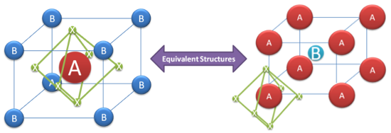
The perovskite lattice arrangement is demonstrated below. As with many structures in crystallography, it can be represented in multiple ways. The simplest way to think about a perovskite is as a large atomic or molecular cation (positively-charged) of type A in the centre of a cube. The corners of the cube are then occupied by atoms B (also positively-charged cations) and the faces of the cube are occupied by a smaller atom X with negative charge (anion).

Depending on which atoms/molecules are used in the structure, perovskites can have an impressive array of interesting properties, including superconductivity, giant magnetoresistance, spin-dependent transport (spintronics) and catalytic properties. Perovskites therefore represent an exciting playground for physicists, chemists and material scientists.
Perovskites were first successfully used in solid-state solar cells in 2012,2,3 and since then most cells have used the following combination of materials in the usual perovskite form ABX3:
- A = An organic cation – methylammonium (CH3NH3+) or formamidinium (NH2CHNH2+)
- B = A big inorganic cation – usually lead(II) (Pb2+)
- X3= A slightly smaller halogen anion – usually chloride (Cl–) or iodide (I–)
Since this is a relatively general structure, these perovskite-based devices can also be given a number of different names, which can either refer to a more general class of materials or a specific combination. As an example of this, we’ve created the table below to highlight how many names can be formed from one basic structure.
| A | B | X3 |
| Organo | Metal | Trihalide (or trihalide) |
| Methylammonium | Lead | Iodide (or triiodide) |
| Plumbate | Chloride (or trichloride) |
The perovskite ‘name-picking’ table: Pick any one item from columns A, B or X3 to come up with a valid name. Examples include: Organo-lead-chlorides, Methylammonium-metal-trihalides, organo-plumbate-iodides etc.
The table demonstrates how vast the parameter space is for potential material/structure combinations, as there are many other atoms/molecules that could be substituted for each column. The choice of material combinations will be crucial for determining both the optical and electronic properties (e.g. bandgap and commensurate absorption spectra, mobility, diffusion lengths, etc). A simple brute-force optimisation by combinatorial screening in the lab is likely to be very inefficient at finding good perovskite structures.
The majority of efficient perovskites are based on Group IV (specifically, lead) metal halides, and moving beyond this has proved challenging. It is likely more in-depth knowledge than currently available is required to fully explore the range of possible perovskite structures. Lead-based perovskite-based solar cells are particularly good because of a range of factors, including strong absorption in the visible regime, long charge-carrier diffusion lengths, a tunable band gap, and easy manufacture (due to the high defect tolerance and the ability to process at low temperatures).